
In this project, your team is going to build a pipelined implementation of AXA, the little instruction set design you built a multi-cycle implementation of in Assignment 2. As in the multi-cycle implementation, here you get to largely ignore reverse execution... however, you will be implementing the undo buffer enough so that all the src operand modes work. In other words, i4$ must be implemented this time.
Remember EE380? Not really? That's ok... just play along anyway. Back in EE380, we followed a rather neat plan in the textbook that basically recommended that a pipelined design could best be created by initially designing a slow single-cycle implementation. The function units, data paths, and control signals defined for the single-cycle implementation could then be used (with only minor modifications) in the pipelined version. It was mostly just a matter of carving the single-cycle design into appropriate pipeline stages... probably about 4 of them. Well, now is the time we see if that approach really works....
I don't suggest that you should take the following diagram too literally.... However, here's a rough diagram showing one way to start thinking about a single-cycle implementation that you can then pipeline:
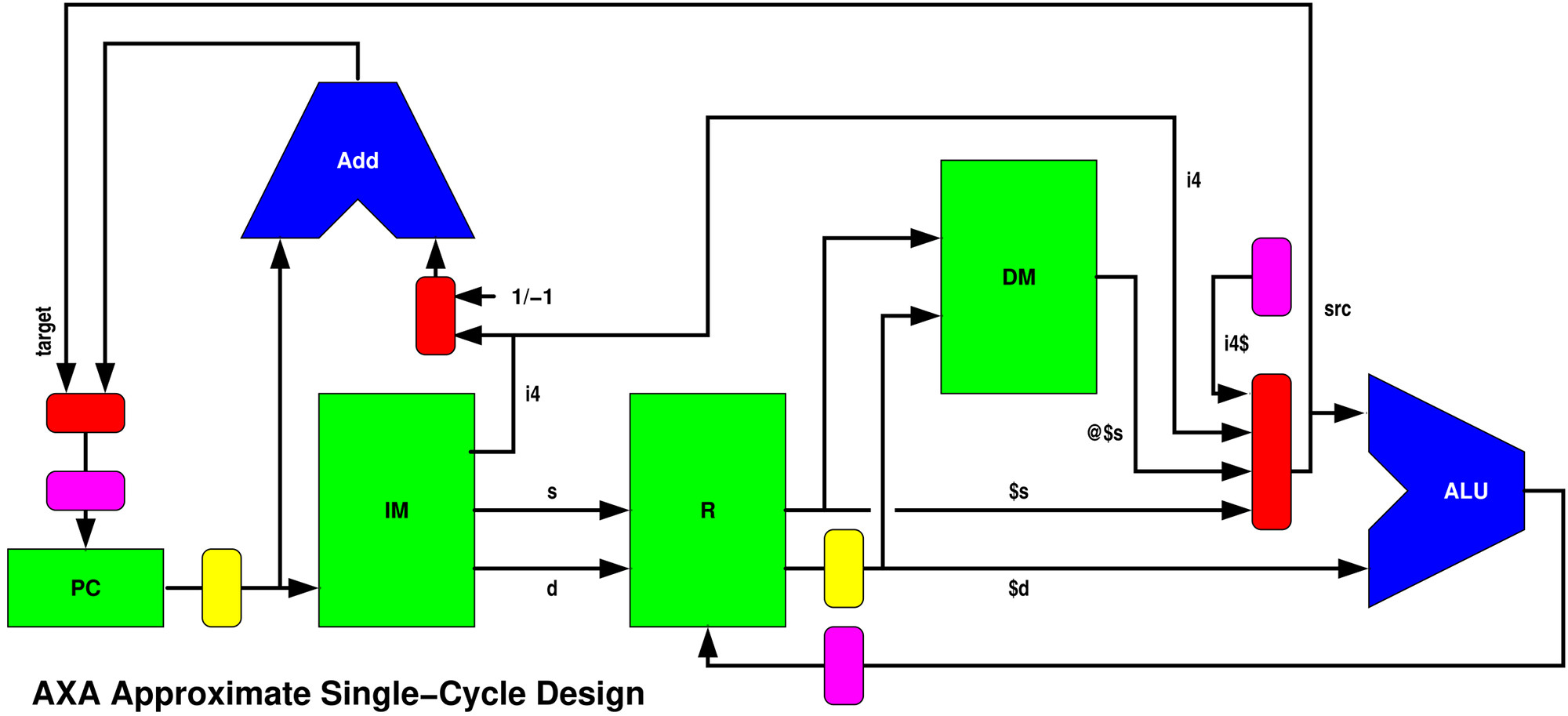
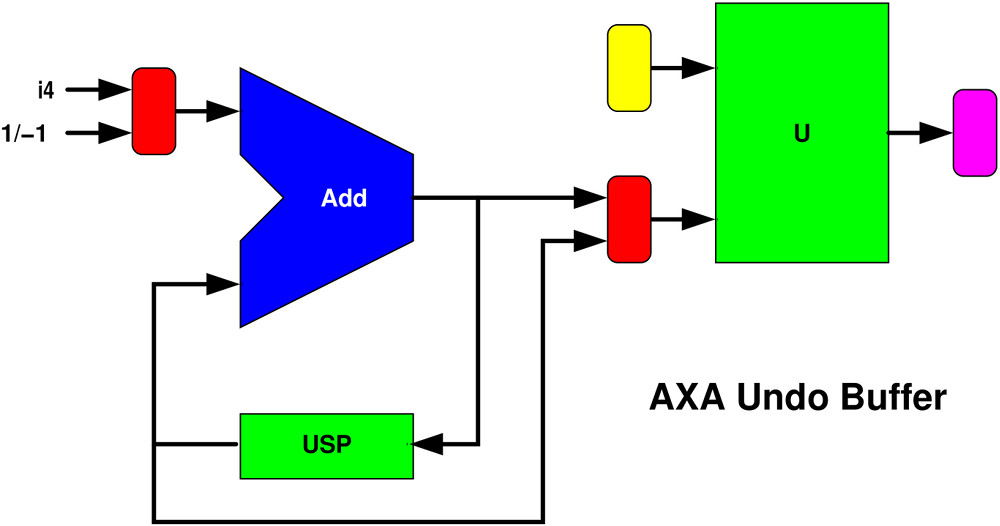
In that diagram, the yellow and magenta blocks are the interface to the undo buffer, which I've drawn separately:
We have been discussing most of the issues in class. I'm not going to go through everything here, but key ideas include:
Well, that wasn't so bad now, was it? Of course, I only gave you an approximate single-cycle design, while you must create a pipelined version.
One of the first steps in making a pipelined implementation is figuring-out how many stages there should be and what belongs in each.
Although we are not forcing you to do any timing analysis, you should make reasonable assumptions about how much can be done in one clock cycle. Your pipelined design most naturally seems to consist of five stages: instruction fetch, register read, data memory access, ALU operation, and register write. Arguably, combining ALU and register write into a single stage might be better. If it makes more sense to you to build greater than five stages, feel free to do that... but I would argue that fewer than four stages would be very difficult to justify. Note that originally I was going to have you deal with the data memory access as two stages sharing hardware: a data read followed by a data write stage. However, only the exchange instruction (ex) writes, and it always writes to the same address as it reads from, so it is quite feasible to design a memory that can do that in one clock cycle.
As we have been discussing in class, one of the most useful concepts in creating hardware (or parallel software) is owner computes: the idea that each register/memory should be written into by only one entity, its owner, and that entity should also compute the value that will be written. Thus, a pipeline doesn't really look at all sequential. Instead, a pipeline is a set of independent, parallel-executing, entities that communicate by the owner of each register updating the register value which is read by one or more other entities. For example, the buffer at the end of the instruction fetch stage (let's call this stage 0) will certainly include a register that holds the destination register number (d), and this "d register" is owned and written by stage 0. Of course, the destination register number is potentially needed until the very last stage (where the register write is done), but it doesn't stay in "d": each stage will have its own register for that. For example, stage one might own "d1" and normally will set it to the value read from "d0". Keep in mind some registers, such as the PC, have many potential sources for their next value -- but the Verilog always block that logically owns the PC is the only thing that should write a new value into it.
Keep in mind that computing complex formulas can be isolated into little always, or combinatorial assign (perhaps even using a Verilog function), blocks that aren't pipeline stages per se. They are parallel-executing hardware units that exist for the sole purpose of owning that computation's result. For example, you might find it easier to have a separate block that owns and computes the interlock condition that would prevent the instruction fetch and register read stages (stages 0 and 1) from advancing when there is a dependence on an instruction further in the pipeline.
Not too bad, right? Well, here are a few more things to think about:
Let's be completely clear about what I expect: your submission should be a viable four-or-more-stage pipelined Verilog implementation of the AXA instruction set implementing complete forward-only (no reverse) execution. The significant design decisions made should also be discussed in your Implementor's Notes.
Assignment 2 was scary, but that was mostly because you had never done something like this before -- now you have. Reusing knowledge and even some code can make this project easier. You are not allowed to use anything from another Assignment 3 team nor from an Assignment 2 team that none of your Assignment 3 team members were on. You can use things done by any of your Assignment 3 team members, including things their teams did on Assignment 2, and things provided as part of this assignment. If you find other materials, for example solutions posted from previous semesters, useful, you may borrow ideas from them, but should generally not literally copy code and you must cite the sources you borrowed ideas from in your Implementor's Notes.
As discussed in class, Verilog code that specifies memory accesses somewhat carelessly is very likely to result in a bigger circuit than if we carefully factored things into modules and created single instances of those modules. For example, a Verilog compiler might fail to map Data Memory into a dedicated memory block within an FPGA, instead constructing a memory using thousands of logic cells. Using an instance of a memory module designed to comply with the FPGA-maker's guidelines (e.g., this dual-port RAM with a Single Clock from ALTERA, which is this Verilog code) ensures that the vendor's Verilog toolchain will correctly infer use of the intended hardware modules inside the FPGA. Incidentally, the ALTERA RAM block seems to be able to handle simultaneous read/write in one clock using the two ports, although the declaration given makes the memory byte-wide rather than storing 16-bit objects. Of course, in this class we are not rendering designs into physical circuits, so these issues of complexity (and timing analysis) are neither obvious nor critical... but you should always be aware of the potential hardware complexity you risk introducing by using a specification style that doesn't explicitly factor-out the desired modules.
Again, the test coverage plan and testbench from Assignment 2 are probably very close to what you want. However, you do need to seriously think about coverage again. Why? You are not testing the same Verilog code, so there may be some paths that didn't exist before -- and they might not be covered with a testbench that covered your old version.
Just to be clear, I do not expect you to incorporate any design for testability features in your Verilog design.
The recommended due date is Friday, November 1, 2019. By that time, you should definitely have at least submitted something that includes the assembler specification (axa.aik), and Implementor's Notes including an overview of the structure of your intended design. That overview could be in the form of a diagram, or it could be a list of top-level modules, but it is important in that it ensures you are on the right track. Final submissions will be accepted up to just before class on Monday, November 4, 2019.
Note that you can ensure that you get at least half credit for this project by simply submitting a tar of an "implementor's notes" document explaining that your project doesn't work because you have not done it yet. Given that, perhaps you should start by immediately making and submitting your implementor's notes document? (I would!)
For each project, you will be submitting a tarball (i.e., a file with the name ending in .tar or .tgz) that contains all things relevant to your work on the project. Minimally, each project tarball includes the source code for the project and a semi-formal "implementors notes" document as a PDF named notes.pdf. It also may include test cases, sample output, a make file, etc., but should not include any files that are built by your Makefile (e.g., no binary executables). Be sure to make it obvious which files are which; for example, if the Verilog source file isn't axa.v or the AIK file isn't axa.aik, you should be saying where these things are in your implementor's notes.
Submit your tarball below. The file can be either an ordinary .tar file created using tar cvf file.tar yourprojectfiles or a compressed .tgz file file created using tar zcvf file.tgz yourprojectfiles. Be careful about using * as a shorthand in listing yourprojectfiles on the command line, because if the output tar file is listed in the expansion, the result can be an infinite file (which is not ok).