In Assignment 2, you defined the instruction encoding, built an assembler, wrote Verilog code for a multi-cycle implementation of the loQ Don instruction set architecture, created a test coverage plan, and tested your design. The good news is that most of that stuff can be reused for this project. The bad news is that you still have a pile of Verilog to write... because you'll be implementing a nice, fast, pipelined version. Qapla'!
Remember EE380? Not really? That's ok... just play along anyway. Back in EE380, we followed a rather neat plan in the textbook that basically recommended that a pipelined design could best be created by initially designing a slow single-cycle implementation. The function units, data paths, and control signals defined for the single-cycle implementation could then be used (with only minor modifications) in the pipelined version. It was mostly just a matter of carving the single-cycle design into appropriate pipeline stages. Well, now is the time we see if that approach really works....
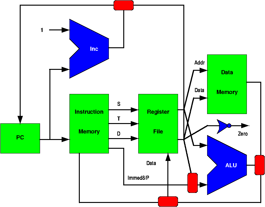
I could ask you to design your own single-cycle implementation from scratch, but I'll save us all some time and give you an overview diagram for such a thing right here:
You should recognize this from my little walk-through in class the week of October 24, but I have re-drawn it much neater. It's also color coded. Registers and other memory units are green, things that compute values are blue, and multiplexors are red. I'm not going to go through everything again here, but some key ideas were:
Well, that wasn't so bad now, was it? Well, of course not... because that's not what you have to do. You have to make a pipelined design.
One of the first steps in making a pipelined implementation is figuring-out how many stages there should be and what belongs in each.
It is fairly obvious that the memories (including the register file) will take a little while to access, and we all know ALUs are notoriously slow. Thus, we'd expect a stage for each of those things along any circuit path. The most natural result is a pipeline with 3 or 4 stages.
See? Now that wasn't so bad, was it? Of course not... but your task is a little harder. The ALU instructions and load and store are all easy, and sys is still just halt, but that leaves three instructions with issues. How can you deal with them?
Let's be completely clear about what I expect: your submission should be a viable three-or-more-stage pipelined Verilog implementation of loQ Don's instruction set. The significant design decisions made should also be discussed in your Implementor's Notes.
Assignment 2 was scary, but that was because you had never done something like this before -- now you have. For this project, you are allowed to reuse any pieces from the Assignment 2 solutions that you, or any of your Assignment 3 teammates. helped create. You also may use any materials I give you here. Perhaps most importantly, you also are free to not use any of those things; in other words, you can combine any of those materials and make changes as your Assignment 3 team sees fit. For example, if you don't like the way instruction fields are encoded, feel free to re-write the AIK assembler (but make sure your Implementor's Notes documents how instructions are encoded and why).
In general, you are not allowed to use anything from another Assignment 3 team nor from an Assignment 2 team that none of your Assignment 3 team members were on. You can use things done by any of your Assignment 3 team members, including things their teams did on Assignment 2, and things provided as part of this assignment.
As discussed in class, Verilog code that specifies memory accesses somewhat carelessly is very likely to result in a bigger circuit than if we carefully factored things into modules and created single instances of those modules. For example, a Verilog compiler might fail to map datamem into a dedicated memory block within an FPGA, instead constructing a memory using thousands of logic cells. Using an instance of a memory module designed to comply with the FPGA-maker's guidelines (e.g., this dual-port RAM with a Single Clock from ALTERA) ensures that the vendor's Verilog toolchain will correctly infer use of the intended hardware modules inside the FPGA. Of course, in this class we are not rendering designs into physical circuits, so these issues of complexity (and timing analysis) are neither obvious nor critical... but you should always be aware of the potential hardware complexity you risk introducing by using a specification style that doesn't explicitly factor-out the desired modules.
Again, the test coverage plan and testbench from Assignment 2 are probably very close to what you want. However, you do need to seriously think about coverage again. Why? You are not testing the same Verilog code, so there may be some paths that didn't exist before -- and they might not be covered with a testbench that covered your old version.
In general, you'd need to write a lot of Verilog code to implement a testbench for a complex circuit. However, as I reminded you in class, here you are building a processor -- so it can actually execute much of its own testing. All we need to do is execute a test program and have code examine the results. This approach has the happy benefit of also being a viable way to test that the actual hardware correctly implements the design: you would just run the code on the actual hardware.
A testbench to execute whatever program until completion is:
module testbench;
reg reset = 0;
reg clk = 0;
wire halted;
processor PE(halted, reset, clk);
initial begin
  $dumpfile;
  $dumpvars(0, PE);
  #10 reset = 1;
  #10 reset = 0;
  while (!halted) begin
    #10 clk = 1;
    #10 clk = 0;
  end
  $finish;
end
endmodule
This just enables trace generation, intializes everything with a reset, and then keeps toggling the clk until the processor says it has reached a halted state.
Next, you need some code to run on it. Running random code might make you feel better, but doesn't test things well and would require that you examine all the memory and register state to see if things worked right. Having your testbench check all memory contents to see if everything is right is awkward because the registers are hidden away inside the processor. However, they are not hidden from code being simulated on the processor, so we could simply add code to check the register values... but then how would I know it succeeded? The answer is a very simple trick: look at where the PC was when it halted (i.e., hopefully when it executed the sys instruction). Simply write code that sequentially tests that each instruction produces the correct result for some inputs, jumping over a sys instruction if each value computed is correct. If the PC ended-up pointing anywhere other than the end of the entire sequence, then from the PC value alone you can tell what instruction failed.
Of course, you can write loQ Don processor code that tests anything -- not just values in registers.
The recommended due date is Monday, November 7 (the anniversary of the Tacoma Narrows Bridge collapse). Final submissions will be accepted up to when class begins on Monday, November 14; this is extended from the original deadline due to a typo in the submission form below that caused project submissions to be rejected.
Each team will submit a project tarball (i.e., a file with the name ending in .tar or .tgz) that contains all things relevant to your work on the project. Minimally, each project tarball includes the source code for the project and a semi-formal "implementors notes" document as a PDF named notes.pdf. (Fairly obviously, the Implementor's Notes should also say who the implementors are -- list all team members as authors.) It also may include test cases, sample output, a make file, etc., but should not include any files that are built by your Makefile (e.g., no binary executables). For this particular project, name the Verilog source file pipe.v.
Submit your tarball below. The file can be either an ordinary .tar file created using tar cvf file.tar yourprojectfiles or a compressed .tgz file file created using tar zcvf file.tgz yourprojectfiles. Be careful about using * as a shorthand in listing yourprojectfiles on the command line, because if the output tar file is listed in the expansion, the result can be an infinite file (which is not ok).
Use the submission form below to submit your project as a single submission for your team -- you do not submit as individuals. The last submission before the final deadline is the one that will be graded.